After four years of 28nm designs, Nvidia recently ushered in the 16nm process by launching today's top performing GPUs: the GeForce GTX 1080 and GTX 1070. In short, their performance was impressive, power consumption was amazing, and prices were... well, typical. Sadly, availability of these new cards has been underwhelming, leaving some consumers frustrated with the temporary hike in pricing.
Those who can afford a $400+ graphics card and actually managed to hunt down a Pascal GPU will no doubt be pleased. For the rest of us, or rather for the majority of us, we have been waiting for something else, and for most that something could be AMD's Radeon RX 480.
Touted as the perfect VR solution for the masses, AMD is hoping to claw back a bit of market share with the new Radeon RX 480 which is aimed at the mainstream $200-250 segment, with other affordable Polaris GPUs expected to follow.
Whether on purpose or forcefully so, AMD is flipping how they used to release new GPUs, starting with mainstream products this time and working up to the high-end stuff. This might make sense given the company's current market share predicament, though I personally feel the move to the 14nm process has almost forced AMD into this strategy. The process may need to mature before larger, more complex GPUs can be created in sufficient volumes.
Then again, with over 80% of the PC gaming market dominated by $100 - $300 graphics cards, this is where the bulk of the market share is won and lost. AMD's first strike will be made at the $200 price range ($240 for the 8GB model) with the RX 480.
This Polaris-based GPU is based on the 4th-generation GCN architecture, boasting up to 15% more performance per Compute Unit (CU) than GPUs using 2nd-gen GCN, according to AMD. Memory performance and compression has also been improved with an updated memory controller supporting GDDR5 at up to 8Gbps data rates for a memory bandwidth of 256GB/s.
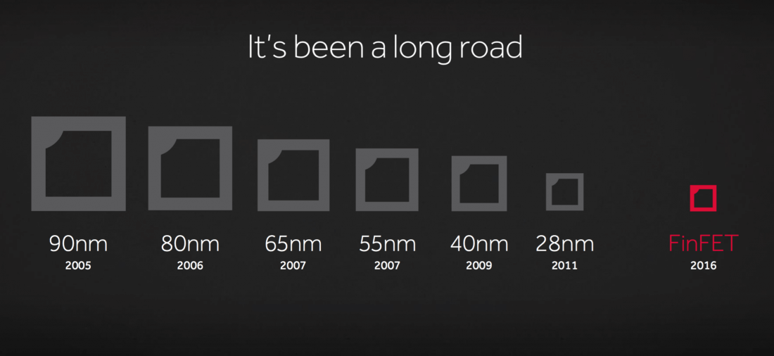
For Polaris, AMD selected Samsung and Global Foundries' 14nm FinFET-based process, which is the densest foundry process available. FinFET transistors are crucial to reducing power consumption and enabling operating voltages that are 150mV lower than the previous generation, thereby cutting active power by 30% from a 1V baseline.
In contrast, Nvidia is using TSMC's 16nm FinFET-based process, so it will be interesting to see how they compare in terms of size and efficiency. Nvidia has had the upper hand in terms of efficiency for some time now and with Pascal proving to be its most efficient architecture yet, we are banking on big things from AMD.
Meet Polaris 10's Biggest GPU
So far we know there will be at least two GPUs based on the Polaris 10 die, the biggest of which is the 2304 Steam Processor-enabled Radeon RX 480.
The die measures just 232mm2, which is incredibly small for a GPU claiming 5.8 TFLOPS of compute power. In terms of physical size, the RX 480 GPU is close to the R7 370, a budget oriented GPU with just 1024 SPUs and 2 TFLOPS of compute power.
| Radeon RX 480 | Radeon R9 390 | GeForce GTX 970 | GeForce GTX 1070 | |
|---|---|---|---|---|
| Release date | June 2016 | June 2015 | September 2014 | May 2016 |
| Price (current) | $240 | $260 | $260 | $400 |
| Price at launch | $240 | $330 | $330 | $380 |
| Architecture | GCN 4th-gen (Polaris) |
GCN 2nd-gen (Polaris) |
Maxwell | Pascal |
| Fab (nm) | 14 | 28 | 28 | 16 |
| Die size (mm2) | 232 | 438 | 398 | 314 |
| Core (MHz) | 1120 | 1000 | 1050 | 1506 |
| Boost (MHz) | 1266 | N/A | 1178 | 1683 |
| Memory (MT/s) | 8000 | 6000 | 7010 | 8000 |
| Cores/TMUs/ROPs | 2304:144:32 | 2560:160:64 | 1664:104:56 | 1920:120:64 |
| Pixel (GP/s) | 81 | 64 | 58.8 | 96.4 |
| Texture (GT/s) | 182.3 | 160 | 109.2 | 180.7 |
| Memory size (MB) | 4096/8192 | 8192 | 3584+512 | 8192 |
| Bus width (bit) | 256 | 512 | 224/32 | 256 |
| Memory type | GDDR5 | GDDR5 | GDDR5 | GDDR5 |
| Bandwidth (GB/s) | 256 | 384 | 196/28 | 256 |
| Single precision (GFLOPS) | 5834 | 5120 | 3494 | 6463 |
| TDP (W) | 150 | 275 | 145 | 150 |
Compared to Nvidia's 16nm Pascal-based GTX 1080 and 1070 GPUs, the Radeon RX 480 is 26% smaller but of course it is targeting a lower performance tier.
Inside that die we have 2304 SPUs, 144 TMUs and 32 ROPs. Core specifications place the RX 480 between the Radeon R9 380X and R9 390. Naturally, it's meant to be more efficient, so that should help it close in on the beefier R9 390. In fact, also helping out here are the advanced clock speeds.
One of the biggest questions surrounding the RX 480 ahead of its launch regarded its operating frequency. The Pascal GPUs run no slower than 1.5GHz and can often be found operating at up to 1.8GHz out of the box using Nvidia's GPU Boost 3.0 technology.
AMD has been more conservative, clocking the Radeon RX 480 at just 1120MHz with a boost clock speed of 1266MHz. This means the RX 480 can operate up to 27% faster than the R9 390 in its stock configuration, which should help compensate for the 10% reduction in cores.
Still, compared to the R9 390, the RX 480 does have one other disadvantage: its memory interface. Even with AMD's generational efficiency improvements, we wonder how they plan to overcome the RX 480's ~30% decrease in memory bandwidth. While the previous generation R9 390 utilized a huge 512-bit wide memory bus allowing 384GB/s of bandwidth using relatively slow 1500MHz GDDR5 memory, the memory bus of the RX 480 has been halved to 256-bit. To close that gap the RX 480 makes use of faster GDDR5 memory clocked at 2000MHz.
We know the RX 480 has fewer cores than the R9 390, but they are clocked a bit higher. We also know that the die is extremely small and that improvements to efficiency have been made beyond the die shrink. All of this helps to explain the card's 150 watt TDP rating, which is some 45% lower than that of the R9 390, though it's concerning that this is the same rating given to the GTX 1070 and we expect that card to be considerably faster.
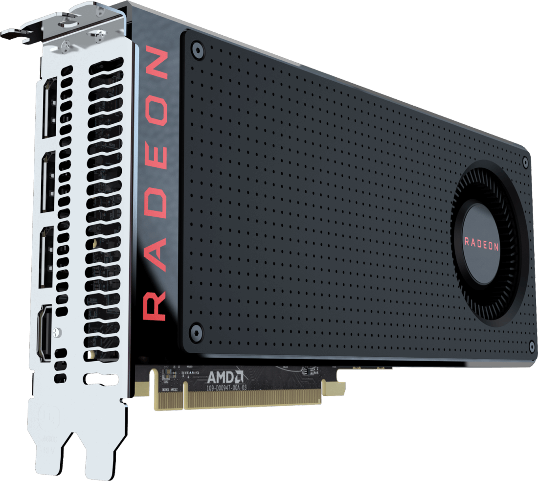
Pricing then will be the Radeon RX 480's key to success. The 8GB model that we are testing tody will cost $240, while a 4GB model will be available for just $200. Both support DirectX 12 along with OpenGL 4.5, OpenCL 2.0 and Vulkan 1.0. They also come with three DisplayPort 1.4 outputs with HDR support and a HDMI 2.0 port supporting 4K @ 60Hz.
AMD Radeon RX 480 'Forefathers Edition'
Unlike Nvidia, AMD won't be charging a premium for graphics cards using its reference cooler. It's also not giving anything a fancy name – the reference card and cooler will be unofficially known as the AMD reference version, just as it has been in the past.
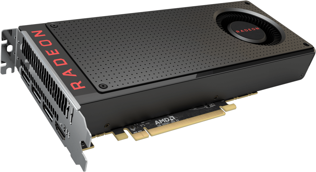
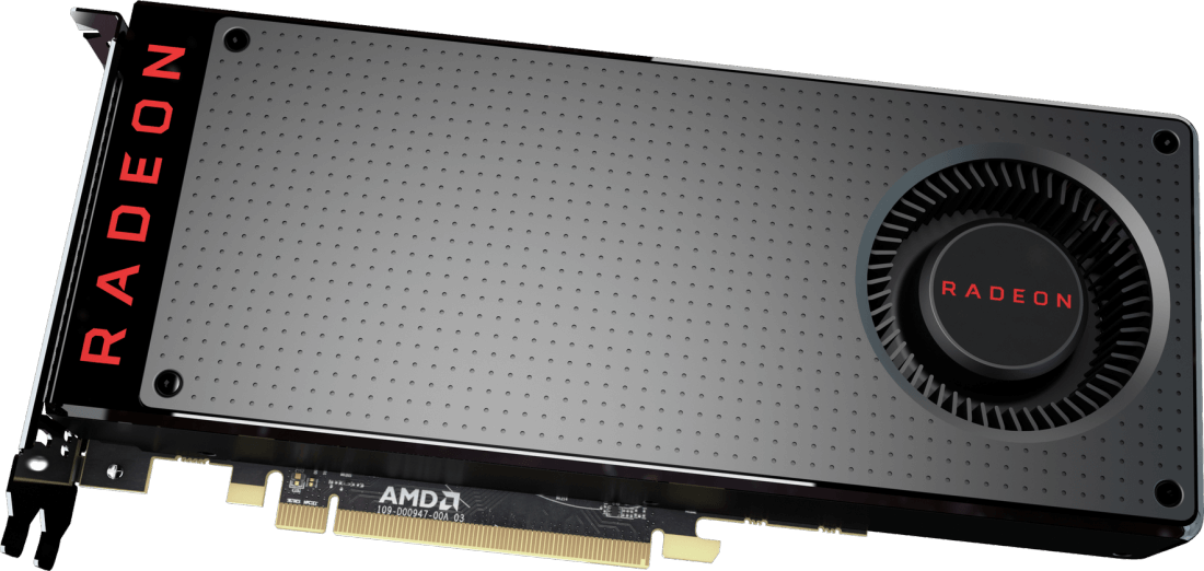
Design-wise the RX 480 reference card is minimalistic, there are no LED lights, no steel fan shrouds and no back plate. Borrowing its design from the previous-gen R9 380, the card looks nice. It has that Fury X look about it, without the liquid cooler hanging out the back. Instead you get a typical blower style fan that can draw in air from both sides, which can be useful in small cases.
The card measures 240mm long, though the PCB is just 177mm, so it should be easy for board partners to produce smaller cards right out of the gate. Whereas most R9 390 cards stretched at least 270mm long, we expect to see most RX 480s shaving 100mm off that length.
The RX 480 reference card is surprisingly light thanks to the use of a very small heatsink. So small that we'd only expected to see this on the lowest end gaming graphics cards. It will be interesting to see how hot the RX 480 runs. We're also curious to see how well the RX 480 overclocks. Considering AMD's recent history, we're not expecting great things, but I am hoping to be pleasantly surprised.
Power consumption should be relatively low going by the TDP rating and the use of a single 6-pin power connector. Even the older R9 380 required two 6-pin connectors, and you had to step down to the R7 370 before you found a single power connector. In fact, the PCB design and configuration looks more like a GeForce GTX 960. Onboard we find a 6+1 phase power design and eight GDDR5 memory chips for a total VRAM capacity of 8GB.
Finally, on to the benchmarks... !
