In brief: At its recent Foundry Forum event, Samsung revealed a fresh roadmap, showing off bleeding-edge process technologies and advanced chip packaging solutions. With breakthroughs in 2nm and 1.4nm processes, the company looks poised to compete with rivals like TSMC amid the generative AI boom.
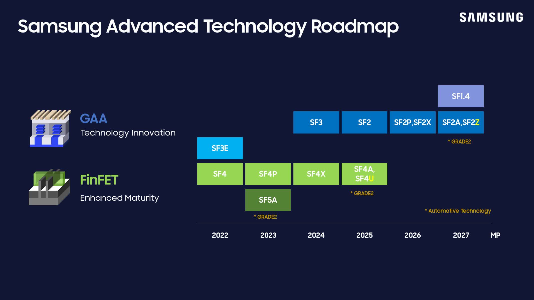
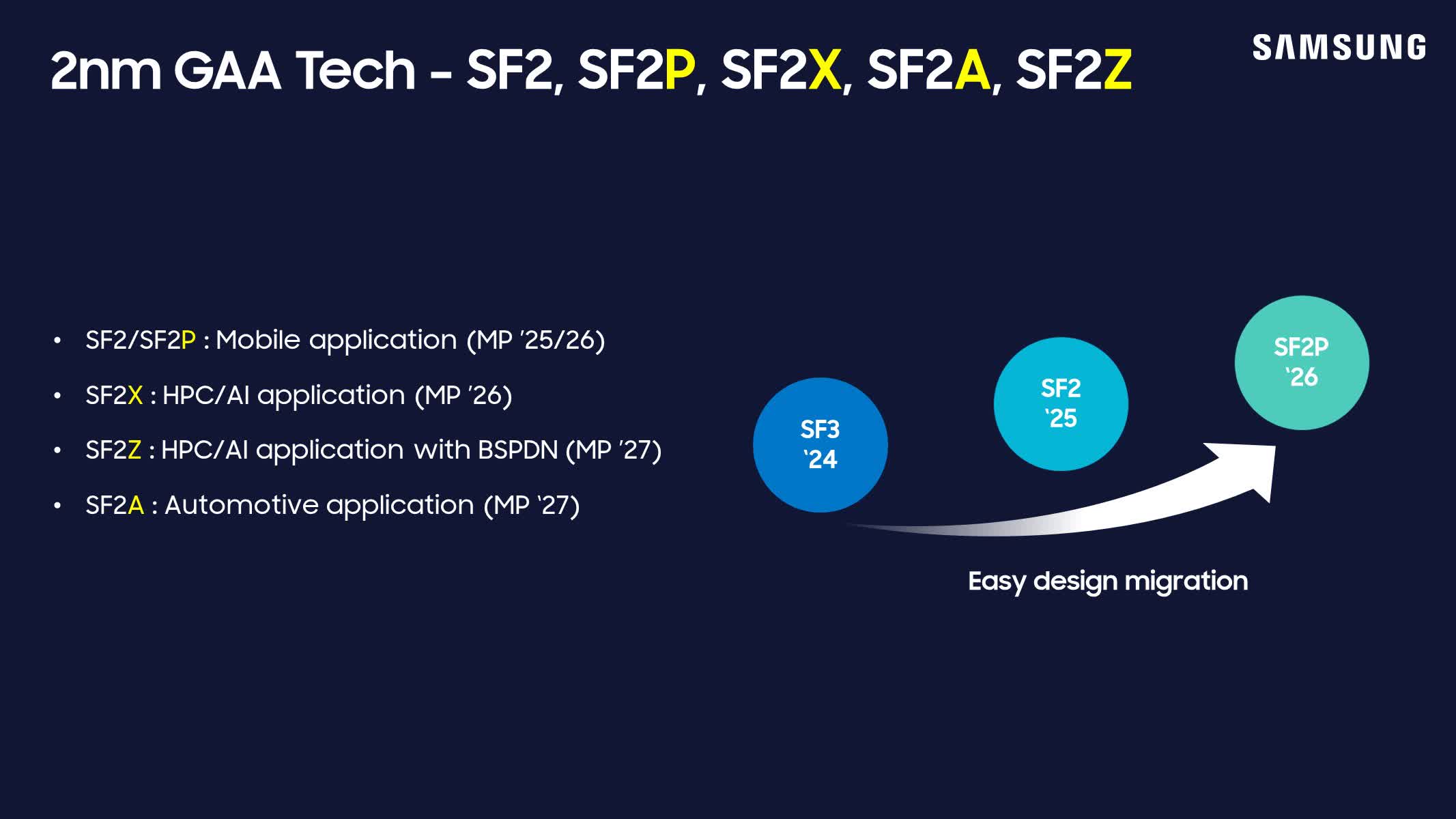
First up, Samsung took the wraps off two new process nodes aimed at pushing the limits of chip performance and efficiency. The headliner is the 2nm SF2Z process, slated for mass production in 2027. This one packs a clever trick with a backside power delivery network (BSPDN) that routes the power rails on the flip side of the silicon wafer. This design eliminates pesky interference issues and voltage drops that hamstring high-performance computing builds.
The SF2Z also brings general PPA (power, performance, area) improvements over Samsung's original 2nm SF2 node. Note that SF2 is the company's second-generation 3nm process rebranded to 2nm, likely created to help it compete better with Intel Foundry. Combined with Samsung's other 2nm nodes, this addition takes the variant count up to five for this fabrication process.

While Samsung markets the SF2 and SF2P nodes for mobile devices, its target audience for SF2X and SF2Z is high-performance computing (HPC). Meanwhile, the final 2nm node will hit automotive applications in 2027. The other new node unveiled is the 4nm SF4U, which uses optical shrinking to boost PPA when it enters mass production in 2025.
Samsung also noted that work on its SF1.4 (1.4nm) process is progressing nicely toward mass production in 2027. However, the company admitted that cracking the sub-1.4nm barrier will require breakthrough material and structural innovations.

One key advantage Samsung is leaning on is its increasing maturity with gate-all-around (GAA) transistors. These 3D transistor structures offer superior switching performance and lower power than traditional FinFET designs. Samsung has been producing GAA chips since 2022 and plans to integrate the technology into its upcoming 2nm process.
Samsung also pulled back the curtain on plans to introduce co-packaged optics (CPO) starting in 2027.
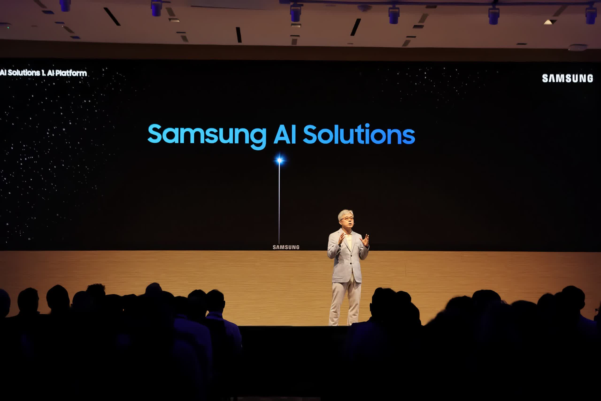
"Alongside our proven GAA process optimized for AI chips, we plan to introduce integrated, co-packaged optics (CPO) technology for high-speed, low-power data processing, providing our customers with the one-stop AI solutions they need to thrive in this transformative era," noted the company in a press release.
Lastly, the company claimed its foundry business has seen AI-related sales surge 80 percent over the past year across various process nodes. That doesn't come as a surprise considering the ongoing AI boom that's benefited other chipmakers, including Nvidia, which recently reported an astonishing 262 percent year-on-year jump in revenue.
